

Overview
In this comprehensive guide, we will explore the process of integrating an ADS1115 16-bit ADC module with the Raspberry Pi Pico, a versatile microcontroller board developed by the Raspberry Pi Foundation. The ADS1115 breakout board is a high-resolution analog-to-digital converter (ADC) that can be used in conjunction with microcontrollers such as Arduino, ESP8266/32, STM32, and of course, the Raspberry Pi Pico.
The Raspberry Pi Pico, powered by the RP2040 microcontroller, offers a built-in 12-bit ADC with a maximum resolution of 3.3V / 4096 = 0.0008V (800uV). While this is an improvement over the Arduino’s 10-bit ADC, it may still be insufficient for projects requiring more precise analog readings. By incorporating the ADS1115 module, which boasts a 16-bit ADC resolution, Pico’s ADC capabilities can be significantly enhanced. With the ADS1115, the smallest voltage that can be measured is 5V / 65536 = 0.000076V (76uV), providing higher precision for your projects. If you want more precison up to 0.3uV, you may check ADS1220 24-Bit ADC Module.
In the following sections, we will discuss the specifications and benefits of the ADS1115 module, outline the required components and connections for integrating it with the Raspberry Pi Pico, and provide a sample MicroPython code to help you get started with this powerful ADC upgrade.
Bill of Materials
To thoroughly understand the ADS1115 ADC Module when used with Raspberry Pi Pico, we require the following components:
| S.N. | Components | Quantity | Purchase Link |
|---|---|---|---|
| 1 | Raspberry Pi Pico | 1 | Amazon | AliExpress |
| 2 | ADS1115 ADC Module | 1 | Amazon | AliExpress |
| 3 | 10K Potentiometer | 1 | Amazon | AliExpress |
| 4 | Breadboard | 1 | Amazon | AliExpress |
| 5 | Connecting Wires | 1 | Amazon | AliExpress |
ADS1115 Chip
The ADS1115 is a precision, low-power, 16-bit, I2Ccompatible, analog-to-digital converter IC.

Features of ADS1115
- 16-bit Resolution
- Four (4) Channel Single-Ended or Two (2) Channel Differential Inputs
- I2C Protocol Interface
- Programmable Comparator
- Wide Supply Range
- Low Current Consumption
- Continuous-Conversion Mode
- Programmable Data Rate
- Programmable Comparator
- Single-Cycle Settling
- Internal Low-Drift Voltage Reference
- Internal Oscillator
- Wide Operating Temperature Range
- Available in Ultra-Small X2QFN Package
ADS1115 Pin Configuration
The below image shows the pin configuration of the ADS1115 chip.

- Pin 1 is the ADDR pin that selects the I2C address for the chip.
- Pin 2 is the Alert/Ready pin which serves as a data ready and alert signal.
- Pin 3 is the GND terminal.
- Pins 4, 5, 6 & 7 are the four (4) ADC input pins. We can use these pins as either four (4) single-ended inputs or two (2) differential inputs.
- Pin 8 is the positive power supply pin which accepts 2.0 V to 5.5 V
- Pins 9 and 10 are the terminals for the I2C interface, SDA and SCL respectively.
ADS1115 Functional Block Diagram
The below is the functional diagram for the ADS1115 Chip.

Initially a multiplexer selects the input signal. Then, the selected signal feeds into a Programmable Gain amplifier (PGA). The PGA can be programmed to provide amplification of small signals prior to conversion.
Subsequently, the input is converted by a 16-bit Delta Sigma converter. The converter uses its own built-in voltage reference and built-in oscillator in measuring the input signal. Finally, the result of the conversion goes into the I2C interface. Also, a comparator provides a signal to the external interface that the result is ready for fetching.
Typical Connections of the ADS1115
The principle I2C connections for the ADS1115 is shown in the image below.

The ADS1115 interfaces directly to standard mode, fast mode, and high-speed mode I2C controllers. Any microcontroller I2C peripheral, including master-only and single-master I2C peripherals, operates with the ADS1115.
For more information refer to ADS1115 Datasheet
ADS1115 Module or Breakout Board
The ADS1115 comes with X2QFN & VSSOP package which can’t be used for prototyping. Therefore we need the ADS1115 Module or Breakout Board to use it with Raspberry Pi Pico or Any other Microcontroller.

These modules are widely available from different manufacturers and are very inexpensive. They are breadboard friendly and can be easily used in prototyping and testing applications.
ADS1115 Module Pinout
The ADS1115 Module has a total number of 10 Pins.
| Pin. No. | Pin Name | Pin Description |
| 1 | VDD | Power supply: 2.0V to 5.5V |
| 2 | GND | Ground |
| 3 | SCL | Serial clock input: Clocks data on SDA (used for I2C communication) |
| 4 | SDA | Serial data: Transmits and receives data (used for I2C communication) |
| 5 | ADDR | I2C address select (slave) |
| 6 | ALERT/RDY | Digital comparator output or conversion ready |
| 7 | AIN0 | Differential channel 1: Single-ended channel 1 input or Negative input |
| 8 | AIN1 | Differential channel 1: Single-ended channel 2 input or Negative input |
| 9 | AIN2 | Differential channel 2: Single-ended channel 3 input or Positive input |
| 10 | AIN3 | Differential channel 2: Single-ended channel 4 input or Negative input |
ADS1115 Module Schematic
The schematic diagram shown above is Adafruit’s version of the ADS1115 module.

It follows the typical connection for the ADS1115 chip. The 10K ohms pull-up resistors are installed on the I2C and Alert pins. Also, there is a 1uF capacitor installed between the VDD pin and the GND which serves as a decoupling capacitor.
How to use ADS1115 Module with Raspberry Pi Pico
Interfacing an ADS1115 module with a Raspberry Pi Pico is straightforward, as both devices use the I2C communication protocol. In this tutorial, we will guide you through the steps to connect and configure the ADS1115 with the Raspberry Pi Pico.

- Connect the VCC pin of the ADS1115 to the 3.3V pin (Pin 36) of the Raspberry Pi Pico.
- Connect the GND pin of the ADS1115 to any GND pin on the Raspberry Pi Pico (e.g., Pin 38).
- Connect the SDA pin of the ADS1115 to the SDA (GP14, Pin 19) pin of the Raspberry Pi Pico.
- Connect the SCL pin of the ADS1115 to the SCL (GP15, Pin 20) pin of the Raspberry Pi Pico.

You may connect the A0, A1, A2, and A3 pins of the ADS1115 to the sensors or devices whose analog values you want to read. In this example, we will use a 10K Potentiometer.
MicroPython Code/Program
Now let us write a MicroPython Code to read ADC Value from ADS1115 connected to Raspberry Pi Pico.
The code doesn’t require any libraries. Hence you can copy the following code and paste it to the Thonny Editor. Save the file with name main.py.
|
1 2 3 4 5 6 7 8 9 10 11 12 13 14 15 16 17 18 19 20 21 22 23 24 25 26 27 28 29 30 31 32 33 |
import utime from machine import I2C, Pin dev = I2C(1, freq=400000, scl=Pin(15), sda=Pin(14)) devices = dev.scan() for device in devices: print(device) address = 72 def read_config(): dev.writeto(address, bytearray([1])) result = dev.readfrom(address, 2) return result[0] << 8 | result[1] def read_value(): dev.writeto(address, bytearray([0])) result = dev.readfrom(address, 2) config = read_config() config &= ~(7 << 12) & ~(7 << 9) config |= (4 << 12) | (1 << 9) | (1 << 15) config = [int(config >> i & 0xff) for i in (8, 0)] dev.writeto(address, bytearray([1] + config)) return result[0] << 8 | result[1] def val_to_voltage(val, max_val=26100, voltage_ref=3.3): return val / max_val * voltage_ref print(bin(read_config())) while True: val = read_value() voltage = val_to_voltage(val) print("ADC Value:", val, "Voltage: {:.3f} V".format(voltage)) utime.sleep(0.5) |
Code Explanation
|
1 2 |
import utime from machine import I2C, Pin |
These lines import the utime, I2C, and Pin modules.
|
1 |
dev = I2C(1, freq=400000, scl=Pin(15), sda=Pin(14)) |
This line initializes the dev variable as an instance of the I2C class, which is used to communicate with I2C devices. It is initialized with the parameters: 1 as the bus number, 400000 as the communication frequency, Pin(15) as the pin for the clock line (SCL), and Pin(14) as the pin for the data line (SDA).
|
1 2 |
devices = dev.scan() for device in devices: print(device) |
These lines scan the I2C bus using the scan() method of the I2C class and print out the addresses of all devices that respond.
|
1 |
address = 72 |
This line sets the address variable to the address of the ADC.
|
1 2 3 4 |
def read_config(): dev.writeto(address, bytearray([1])) result = dev.readfrom(address, 2) return result[0] << 8 | result[1] |
This function sends a bytearray containing a 1 to the ADC at the specified address, which sets the ADC to the configuration mode and prepares it to receive configuration data. The dev.readfrom() method then reads two bytes of data from the same address, which are combined into a single 16-bit integer using bitwise operations (<< and |). This integer represents the configuration settings for the ADC and is returned.
|
1 2 3 4 5 6 7 8 9 |
def read_value(): dev.writeto(address, bytearray([0])) result = dev.readfrom(address, 2) config = read_config() config &= ~(7 << 12) & ~(7 << 9) config |= (4 << 12) | (1 << 9) | (1 << 15) config = [int(config >> i & 0xff) for i in (8, 0)] dev.writeto(address, bytearray([1] + config)) return result[0] << 8 | result[1] |
This function is used to read the actual analog voltage data. It first sends a bytearray containing a 0 to the ADC at the specified address, which puts the ADC into conversion mode and starts the conversion process. It then reads two bytes of data from the same address using the dev.readfrom() method and combines them into a single 16-bit integer. The read_config() function is called to retrieve the current configuration settings for the ADC, which are then modified using bitwise operations (& and |) to set the conversion mode to single-ended and to select the input channel. The modified configuration settings are then converted to a bytearray and sent to the ADC using the dev.writeto() method. The function then returns the converted voltage value.
|
1 2 |
def val_to_voltage(val, max_val=26100, voltage_ref=3.3): return val / max_val * voltage_ref |
This function converts the raw ADC value to a voltage value using the provided maximum value and voltage reference.
|
1 |
print(bin(read_config())) |
This line prints the binary representation of the current configuration settings for the ADC.
|
1 2 3 4 5 |
while True: val = read_value() voltage = val_to_voltage(val) print("ADC Value:", val, "Voltage: {:.3f}V".format(voltage)) utime.sleep(0.5) |
This is the main loop that continuously reads the ADC value using the read_value() function and converts it to a voltage value using the val_to_voltage() function. It then prints the converted values to the console and waits for half a second using the utime.sleep() function. The loop continues indefinitely until the program is stopped manually.
Testing & Demo
Run the code. If all connections are correct, the terminal will show the ADC Value and the voltage value.
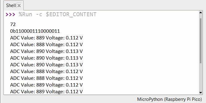
The minimum voltage observed was 0V which has the ADC value of 1-2 or almost 0.
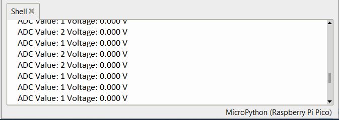
The maximum value shown was almost 3.3V which shows the maximum ADC value of 26091.
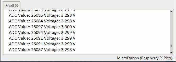
Thus we can conclude that the ADS1115 16-Bit ADC Module has good accuracy and can be used for multipurpose applications. You may use a ADC Calculator to manually calculate the ADC Value.
According to other tests, this device has a stated typical accuracy of 0.01% but it has a maximum accuracy of 0.15%. This accuracy includes all sources of error such as voltage reference, Gain error, offset, and noise.
Video Tutorial & Guide

The same ADS1115 Module can also be used with other Microcontrollers which are as follows:


2 Comments
Excellent document.
I have a question.
If it is 16 bits, why 26100 and not 65535?
How to read channel 0 and 1?
Thank you so much.
You have a point. The ADS1115 has its own reference voltage. The constant in the calculation of the measured raw voltage depends only on the voltage Full-Scale Range (FSR) specified in the condition register of the ADS1115, independently of the supply voltage. This is in contrast to the Arduino ADC. See data sheet ADS1115 (Ti.com).
For the excellently documented code of all AD1115 functions see: https://github.com/wollewald/ADS1115_mpy