

Overview
In this guide, we will design Negative Voltage Generator Circuit using a 555 Timer IC. Negative voltage, in the context of electrical circuits, refers to a voltage that is lower than the reference ground potential. In other words, when a certain point in a circuit has a voltage level below the ground or 0V, it is considered a negative voltage.
A negative voltage generator circuit can be designed using a 555 timer IC in conjunction with other passive components. The 555 timer IC is a versatile component that can be used in various configurations, such as astable, monostable, and bistable multivibrators. In this case, we’ll use the 555 timer in an astable configuration to generate a square wave, which will then produce a negative voltage with the help of a diode-capacitor voltage doubler.
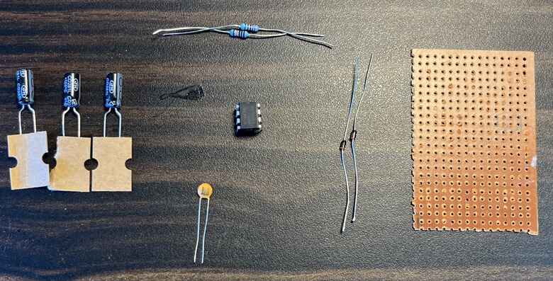
Components Required
- 555 timer IC
- Resistors: R1 = 1kΩ, R2 = 10kΩ
- Capacitors: C1 = 10uF, C2 = 10uF, C3 = 0.1uF
- Diodes: D1, D2 (1N4148 or 1N4007)
- 2 Pin Terminal Block – 2 Qt
- 9V battery or equivalent power supply
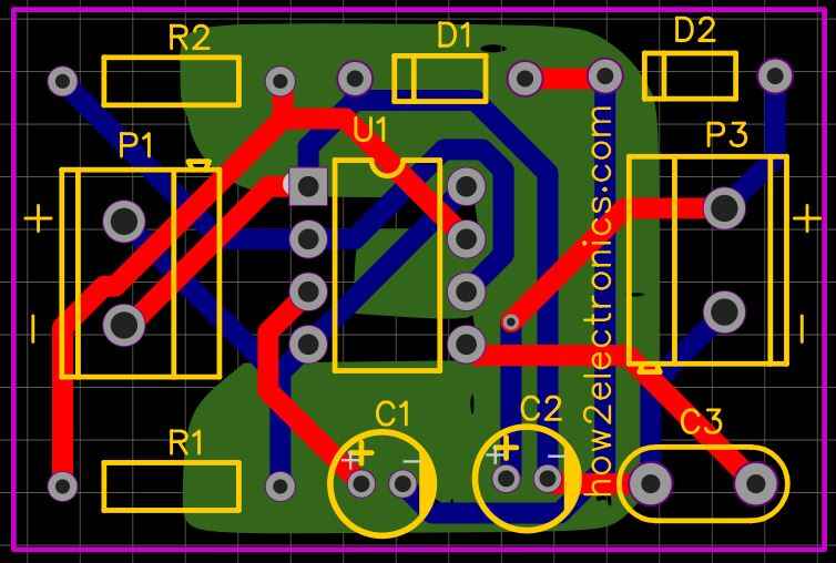
Circuit Diagram & PCB Design
The following is the circuit diagram of the Negative Voltage Generator Circuit using 555 Timer IC. The circuit is very simple.

The 555 Timer IC is configured in Astable Multivirabtor Mode.
Here is the PCB for this project designed using EasyEDA Software.
The Gerber File for the PCB is useful in manufacturing the PCB.
This is the 3D view of the PCB which looks awesome.
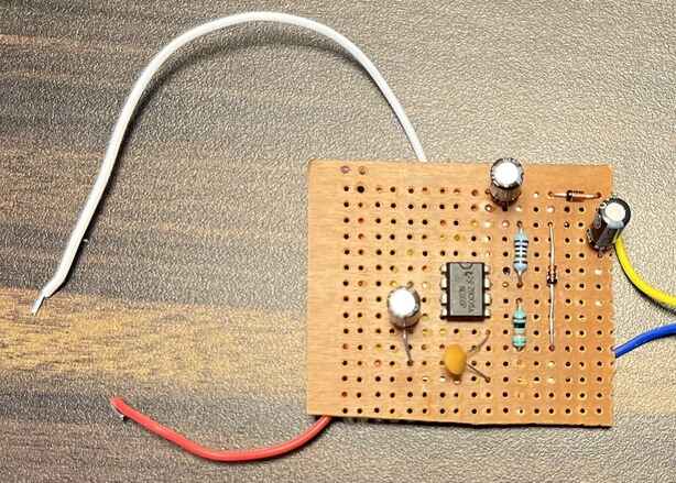
For testing purposes I used Vero Board and assembled all the components there.
Working of Negative Voltage Generator Circuit using 555 Timer
The negative voltage generator circuit utilizes a 555 timer IC configured in astable mode to produce a continuous square wave output at pin 3. The frequency and duty cycle of this square wave are determined by the resistor and capacitor values (R1, R2, and C3). As the square wave oscillates between high and low states, the capacitors C1 and C2 undergo charging and discharging cycles, which are essential to the generation of a negative voltage across capacitor C2.
The process of charging and discharging capacitors, known as charge pumping, occurs through diodes D1 and D2. When the output at pin 3 is high, diode D1 becomes forward-biased, allowing current to flow and charge capacitor C2. Conversely, when the output is low, diode D2 is forward-biased, allowing the charged capacitor C2 to discharge, creating a negative voltage across it.
Overall, the circuit generates a negative output voltage based on the value of R1 & R2 but with opposite polarity. However, due to diode voltage drops and other losses, the output voltage may be slightly lower than the input voltage.
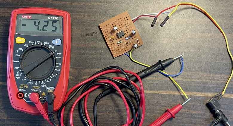
Please note that this circuit can provide only a small amount of current (a few milliamperes) and is suitable for low-power applications. If you need a higher current, you may need to consider using a different approach, such as a charge pump or a switching regulator with an inductor.


