
")
Overview:
In this project, we will build a DIY 5V 3A USB Charger designed specifically for cars or solar panels using the NS6326B IC. This versatile charger is engineered to accept a wide input voltage range of 4-30V, making it highly adaptable to various power sources, from automotive batteries to solar-generated electricity. The NS6326B IC at its core ensures efficient voltage regulation and stable power delivery, ensuring your devices receive a consistent 5V output.
The charger boasts features like over-voltage protection, current sampling, and a robust power switch output mechanism, ensuring safety and reliability in diverse environments. Its 3A output capability ensures rapid charging for most USB-powered devices, from smartphones to tablets. Given its flexibility in input voltage and compact design, this charger is ideal for on-the-go applications, be it in cars, RVs, or remote locations powered by solar panels.
Bill of Materials
The following are the components required to make a 5A 3A USB Charger Circuit.
| S.N. | Components | Quantity | Purchase Link |
|---|---|---|---|
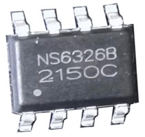
| 1 | NS6326 IC | 1 | AliExpress |
| 2 | 100uF/35V electrolytic capacitor | 1 | AliExpress |
| 3 | 470uF/16V electrolytic capacitor | 1 | AliExpress |
| 4 | 0.1uF Capacitor 0805 | 1 | AliExpress |
| 5 | 47uH Inductor | 1 | AliExpress |
| 6 | USB Type A Port Female | 2 | AliExpress |
| 7 | LED 0805 (Red) | 1 | AliExpress |
| 8 | Resistor 0805 (220-ohm) | 1 | AliExpress |
NS6326B 4-30V Input 5V/3A Output Synchronous Buck Regulator
The NS6326B is a synchronous buck power management chip that supports high-voltage inputs. It can achieve a continuous current output of 3A within a wide input voltage range of 4~30V.
The NS6326B has excellent constant voltage/constant current (CC/CV) characteristics. It uses a current mode loop control principle to achieve a fast dynamic response. The NS6326B operating switching frequency is 130kHz, which has good EMI characteristics. Additionally, the chip includes multiple protection functions: over-temperature protection, output short circuit protection, and input under-voltage/over-voltage protection. The NS6326B uses a standard SOP8 package.
Features of NS6326B
- Wide input voltage range: 4V to 30V
- Efficiency up to 92% and above
- High constant current accuracy: ±5%
- Constant voltage accuracy: ±5%
- No external compensation required
- Switching frequency: 130kHz
- Input under-voltage/over-voltage, output short circuit, and overheat protection
- SOP-8 package
- Output current: 3A
Pin Configuration
The SOP-8 pin diagram is shown, detailing the functions of each pin.
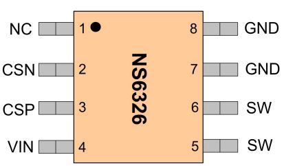
| Pin Number | Pin Name | Description | Function |
|---|---|---|---|
| 1 | NC | Floating Pin | – |
| 2 | CSN | Output Voltage | Output voltage pin |
| 3 | CSP | Current Sampling Pin | This pin is used to detect and set the output constant current value; the size of the output constant current value is set by R3: ICC-Mode = Vcs/R3 |
| 4 | VIN | Power Supply | Power supply pin, this pin should be connected to at least a 100uF/35V electrolytic capacitor to the ground to avoid large voltage fluctuations at the input during operation |
| 5,6 | SW | Power Switch Output | This pin is the switch node, connected to the inductor, used for power output to the load |
| 7,8 | GND | Ground | Ground pin |
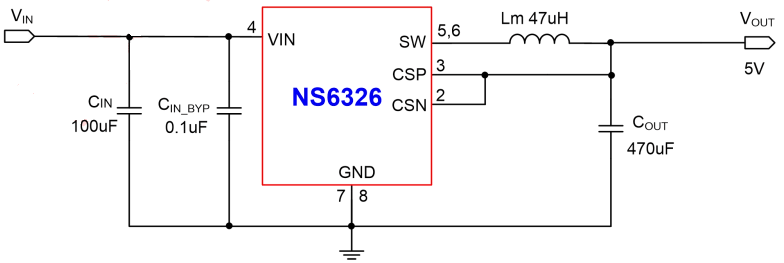
NS6326B Typical Application Circuit
Application Range
- Car chargers/adapters
- Linear regulator pre-regulators
- Distributed power systems
- Battery chargers
5V 3A USB Charger Circuit
Let us take a look at the 5V 3A USB Charger Circuit for a Car or Solar Panel. The schematic is modified from the NS6326B Typical Application Circuit.

In this schematic, the terminal J1 can be used for power input which can range from 4-30V. The input source could be a 12V Battery or a DC Adapter Supply. The input could also be a 24V Solar Panel.
The output can be taken from a pair of Male USB A ports. A terminal J2 is also provided so that a header or a jumper wire can be soldered to take power input.
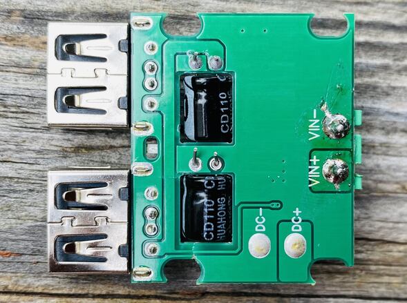
Using the above schematic, you can design your own custom PCB. I used PCB for my project and soldered all the necessary components on it.

All the components on the front side and back side are soldered as per the circuit diagram.
Testing & Operations
After assembling the hardware, you can start testing the PCB Board. You may connect a 12V Lead-Acid Battery at Input terminal.
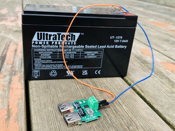
The on-board LED on the board will turn on indicating the board is powered on. You may use a multimeter to check the input and the output voltage.
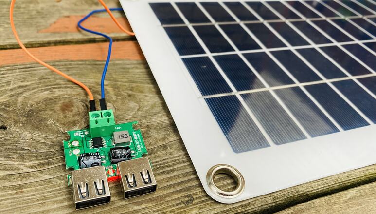
Similarly, instead of 12V DC Battery, you may connect a 24V Solar Panel.
You can charge your mobile phone using the USB Port.
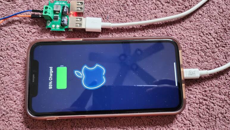
The 5V 3A USB Charger can be useful is so many other applications that requires constant power source.


