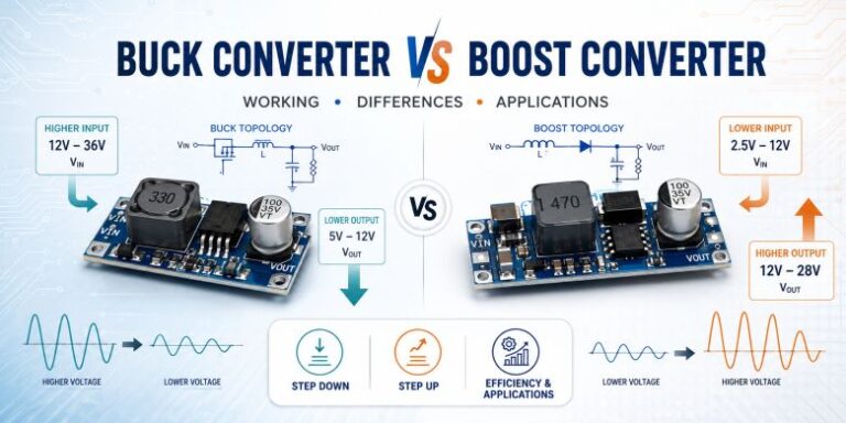
Overview: Buck Converter vs Boost Converter
Buck and boost converters are two of the most important DC–DC converter topologies used in power electronics. A buck converter reduces voltage, while a boost converter increases it. However, the practical choice involves more than voltage conversion alone: current waveforms, ripple, control-loop behavior, efficiency, electromagnetic interference, thermal stress, and component ratings all matter.
Buck Converter Working
A buck step-down) converter uses a switching device—usually an N-channel MOSFET—together with a diode or synchronous MOSFET, an inductor, and an output capacitor. Its purpose is to convert a higher DC input voltage into a lower regulated output voltage.
In continuous conduction mode (CCM), the switch alternates between two states:
- Switch ON: The input is connected to the inductor. The inductor current rises with an approximate slope of (Vin − Vout)/L, storing energy in the magnetic field.
- Switch OFF: The inductor continues supplying current through the diode or low-side MOSFET. The inductor current falls with an approximate slope of Vout/L.
Vout ≈ D × VinAt steady state, the inductor volt-seconds balance over one switching period. The output LC filter smooths the triangular inductor current, so the load receives an almost continuous current. In contrast, the input current is pulsed because the source is connected to the switching stage only during the ON interval.
Ripple and EMI in a Buck Converter
The pulsed input current produces high di/dt at the input. Without correct bypassing, this creates voltage ripple, ringing, and electromagnetic interference on the supply side. A low-ESR input capacitor must therefore be placed very close to the MOSFET and return path to keep the high-frequency current loop small.
The output side usually has lower ripple because the inductor and output capacitor form a low-pass filter. A low-ESR capacitor near the inductor and rectifier reduces output ripple and supports the load during switching transitions.
Efficiency and High-Current Operation
Practical buck-converter losses include MOSFET on-resistance, inductor winding resistance, diode forward drop, switching transitions, gate-drive power, and capacitor ESR. Synchronous rectification replaces the catch diode with a MOSFET and is especially useful at moderate or high current because it reduces conduction loss.
At very high output current, multiphase buck converters are common. Two or more interleaved phases divide the load between parallel inductors and switches. This reduces ripple per phase, distributes heat, and lowers electrical stress on individual components.
Control-Loop Behavior
A buck converter has relatively straightforward control dynamics in CCM. It does not contain the right-half-plane zero that complicates boost-converter control. As a result, a properly compensated buck controller can use a comparatively high loop bandwidth and respond quickly to changing loads.
High duty cycles approaching 95–99% are possible with suitable high-side gate-drive circuitry, although bootstrap drivers generally require the duty cycle to drop periodically so the bootstrap capacitor can recharge.
Boost Converter Working
A boost (step up) converter uses a switch, inductor, diode, and output capacitor to produce an output voltage greater than the input voltage.
Its two switching states are:
- Switch ON: The switch connects the inductor to ground. Inductor current rises with an approximate slope of Vin/L, and energy is stored in the inductor.
- Switch OFF: The inductor voltage reverses and adds to the input voltage. Current flows through the diode into the output capacitor and load.
Vout = Vin / (1 − D)In other words, as the duty cycle D approaches 1, the boost converter can produce arbitrarily higher outputs (limited in practice by switch/node voltage ratings, saturation, and control).
Ripple and Current Waveforms
The boost converter has a continuous, triangular input current because the inductor is in series with the source. Its output current is pulsed because energy reaches the output primarily during the switch-OFF interval. The output capacitor must supply the load between these pulses, so output ripple is generally more significant than input ripple.
This behavior is the opposite of a buck converter: a buck has pulsed input current and comparatively smooth output current, while a boost has smoother input current and pulsed output current.
Protection and Component Stress
The input and output of a basic boost converter remain connected through the inductor and diode path. This can make output-short-circuit protection more difficult because current may continue to flow from the source even when the main switch is off.
The boost MOSFET must withstand approximately the full output voltage when it is off. The output rectifier also carries high RMS and peak current during the OFF interval. Synchronous rectification can improve efficiency at higher current by replacing the diode with a controlled MOSFET.
Right-Half-Plane Zero
A major control challenge in a CCM boost converter is the right-half-plane (RHP) zero. When the duty cycle is increased, the converter initially stores more energy in the inductor and delivers less energy to the output. The output voltage may therefore dip briefly before it rises.
fRHP = Rload(1 − D)2 / (2πL)The RHP zero introduces phase lag and limits achievable loop bandwidth. Designers commonly keep the closed-loop crossover frequency well below the RHP-zero frequency—often around 10–20% of it—to preserve stability. This makes a boost converter slower to recover from sudden load changes than a similarly designed buck converter.
Voltage-mode and current-mode boost controllers therefore require careful compensation. At light load, the converter may enter discontinuous conduction mode, changing the small-signal behavior and compensation requirements.
Direct Technical Differences
1. Step-Down vs Step-Up Operation
A buck converter produces an output below the input, with an ideal gain of D. A boost converter produces an output above the input, with an ideal gain of 1/(1 − D). Both expressions assume ideal components and continuous conduction.
2. Current-Waveform Behavior
In a buck converter, the inductor is on the output side, so output current is nearly continuous while input current is pulsed. In a boost converter, the inductor is on the input side, so input current is nearly continuous while output current is pulsed through the rectifier.
3. Control Complexity
Buck converters are minimum-phase systems in CCM and are normally simpler to compensate. Boost converters contain an RHP zero, which forces a lower loop bandwidth and adds control complexity.
4. Efficiency Behavior
Both topologies can reach high efficiency, especially with synchronous rectification. A buck converter generally performs very well at high current and large step-down ratios. A boost converter may experience greater current and switching stress at high duty cycle, particularly when the required voltage gain is large.
Neither topology is automatically more efficient in every case. Efficiency depends on duty cycle, switching frequency, MOSFET RDS(on), diode loss, inductor DCR, gate charge, load current, and PCB thermal performance.
5. EMI and Filtering
A buck converter has its strongest switching ripple at the input, so its input capacitor and high-current switching loop require close attention. A boost converter has relatively smooth input current but pulsed current at the output, so the diode, output capacitor, and switch-node loop are major EMI concerns.
6. Component Stress
In a buck converter, the main switch generally blocks the input voltage. In a boost converter, the main switch generally blocks the output voltage, which may be much higher. The boost inductor and switch can also carry substantially more current than the output load current when the duty ratio is high.
Buck vs Boost Converter Comparison Table
| Parameter | Buck Converter | Boost Converter |
|---|---|---|
| Main function | Steps voltage down | Steps voltage up |
| Ideal CCM gain | Vout ≈ D × Vin | Vout = Vin/(1 − D) |
| Input current | Pulsed | Continuous and triangular |
| Output current | Nearly continuous | Pulsed |
| Dominant ripple location | Input side | Output side |
| Control dynamics | Relatively simple; no CCM RHP zero | More difficult; CCM RHP zero limits bandwidth |
| Switch voltage stress | Approximately input voltage | Approximately output voltage |
| Typical transient response | Faster and easier to optimize | Slower due to bandwidth limitations |
| Common applications | Processor rails, automotive logic rails, embedded power, low-voltage LED loads | Battery-to-USB power, LED strings, bias rails, 3.3 V to 5 V conversion |
Design Implications
Inductor Selection
The inductor determines the ripple-current amplitude and strongly affects conduction mode, transient response, physical size, and efficiency. A larger inductance produces lower ripple and maintains CCM over a wider load range, but it is usually larger and can slow the converter response.
A common starting target is a peak-to-peak inductor ripple current of approximately 20–40% of the average inductor current. For a boost converter, a commonly used first-order expression is:
L = Vin × D / (fsw × ΔIL)The selected inductor must also have sufficient saturation-current rating, low DCR, and acceptable core loss at the chosen switching frequency.
Control Bandwidth and Transients
A buck converter can often use a control bandwidth approaching roughly one-tenth of the switching frequency when the controller and power stage allow it. This makes it well suited to loads with abrupt current changes.
A boost converter must normally use a much lower crossover frequency because of the RHP zero. Designers may use feed-forward control, peak-current-mode control, sufficient output capacitance, or carefully shaped compensation to improve transient behavior without sacrificing stability.
Synchronous Rectification
Replacing a diode with a synchronous MOSFET can substantially reduce conduction loss at moderate and high current. The benefit must be balanced against MOSFET gate-charge loss, driver complexity, dead-time control, and body-diode conduction.
Too much dead time increases diode conduction loss, while too little dead time can cause both MOSFETs to conduct simultaneously, producing shoot-through current.
Interleaving
Multiphase buck converters are widely used for high-current rails. Interleaving distributes current and heat while reducing net ripple. Interleaved boost converters can reduce input ripple and split peak current between inductors, although phase balancing and control are more complex.
PCB Layout and EMI
High-speed switching requires a compact PCB layout. The highest di/dt loops must be minimized, and ceramic capacitors should be placed directly beside the relevant switching devices.
Buck Layout Priority
Keep the input capacitor, high-side MOSFET, low-side diode or MOSFET, and ground return in a very small loop. Separate the noisy switch node from feedback and analog ground traces.
Boost Layout Priority
Keep the inductor, MOSFET, diode, output capacitor, and return path compact. Minimize switch-node copper area and place the output capacitor close to the diode and load return.
Poor layout can produce ringing, overshoot, unstable feedback, excess radiated emissions, and additional switching loss. RC snubbers or other damping networks may be required in high-power designs.
Thermal Stress
At high current, conduction and switching losses create significant heat. Copper pours, thermal vias, suitable component spacing, and heat sinking may be required. In a boost converter, the output diode or synchronous MOSFET often experiences high pulsed current. In a buck converter, both the high-side and low-side devices carry a large portion of the load current.
Applications
Buck Converter Applications
- Converting 12 V or 5 V to 3.3 V, 1.8 V, or 1.2 V processor rails
- Automotive 12 V battery to 5 V or 3.3 V electronics
- Telecom and server intermediate-bus conversion
- Battery-powered embedded systems
- Low-voltage LED drivers where the supply exceeds the LED-string voltage
- FPGA, CPU, memory, and sensor power supplies
Boost Converter Applications
- Single-cell Li-ion battery to 5 V USB power
- White-LED strings requiring a voltage above the battery rail
- Bias and auxiliary supply rails
- 3.3 V to 5 V conversion for CAN or RS-485 transceivers
- Portable instruments and battery-powered sensors
- Charging and energy-harvesting circuits
How to Choose Between a Buck and Boost Converter
The first decision is based on the complete input-voltage range and the required regulated output voltage.
- Choose a buck converter when Vout is below Vin(min).
- Choose a boost converter when Vout is above Vin(max).
- Choose a buck–boost, SEPIC, or related topology when the input can move both above and below the required output.
Engineer’s Selection Checklist
- Compare voltage ranges: Check minimum and maximum input voltage, not only the nominal value.
- Calculate duty-cycle limits: Very high duty cycle increases current, stress, and loss. A boost duty cycle above approximately 0.85 may justify a different topology.
- Check load dynamics: A buck converter is generally easier to stabilize for fast-changing loads.
- Estimate current stress: In a boost converter, input and inductor current can be much higher than output current.
- Set an efficiency target: Use synchronous rectification when diode loss becomes significant.
- Review ripple sensitivity: Buck ripple is strongest at the input; boost ripple is strongest at the output.
- Check device ratings: Include switching overshoot and thermal derating, not only nominal voltage and current.
- Evaluate EMI and layout: Select a topology whose noisy node is easier to filter in the target system.
- Consider size and cost: Higher inductance, additional filtering, snubbers, synchronous drivers, and multiphase control all affect board area and cost.
Conclusion
Buck and boost converters are simple in principle but behave very differently in real hardware. A buck converter provides efficient step-down conversion, nearly continuous output current, relatively low output ripple, and straightforward control dynamics. A boost converter provides step-up conversion, smoother input current, and the ability to generate a higher rail from a lower source, but its pulsed output current and right-half-plane zero make filtering and control more demanding.
The correct choice depends on the full input and output voltage range, current level, transient requirements, efficiency target, ripple tolerance, thermal limits, EMI goals, component ratings, board area, and cost. In practical terms, use a buck converter for reliable step-down regulation and a boost converter when a stable voltage above the available supply is required.