
 – PCB Design & Analysis")
DFM In PCB Design
The term DFM (Design for Manufacturing) is the process of optimization of a part, product, or component’s design, to create it cheaper and more easily. DFM involves efficiently designing or engineering an object, generally during the product design stage, when it is easier and less expensive to do so, to reduce manufacturing costs. This allows a manufacturer to identify and prevent mistakes or discrepancies. It is a process that enables manufacturers to examine the design of a product in a series of categories to optimize its dimensions, materials, tolerances, and functionality through the most efficient manufacturing means possible. With DFM, certified product contractors scrutinize each new product idea in a range of areas to find the best measurements, materials, and manufacturing processes for the products at hand.
When it comes to designing and producing electronics, success hinges not merely on the excellence of your design, but also on how effectively and efficiently that design can be brought to life. That’s where the concept of DFM comes into play. DFM is the process of designing for ease of manufacturing, and its importance cannot be overstated. Implementing DFM principles from the get-go in your PCB design process can streamline production, mitigate errors, and ultimately save substantial time and money. DFM helps reduce delays caused by defective products, errors and time spent and checking project reviews and documentation.
Goal of DFM
On the other hand, DFM is important in Printed Circuit Boards (PCB), which involve several steps and careful attention to every little detail to avoid issues. Because of that, DFM helps the designers to systemize the PCB Layout design, ensuring that the production process runs error-free and providing certainty about the product quality.
The goal of DFM is to simplify the manufacturing process, reduce production costs, and improve the overall quality of the final product. This involves considering manufacturing constraints and capabilities early in the design phase to minimize complexities, facilitate assembly, and enhance production efficiency. By integrating DFM principles, manufacturers and designers can achieve cost savings, faster time to market, and higher-quality products. DFM occurs early in product development, before tooling and the assembly process, when the product is being designed.
Doing so will make manufacturing less time-consuming, which will reduce cost and increase the ease of manufacturing. The exact process of DFM will depend on what product is being designed and produced. General principles of DFM include designing objects for efficient assembly, the standardization of materials and components, reducing the number of parts, and minimizing the amount of manufacturing operations required on parts during assembly. Other basics of effective DFM include standardization of parts to save on part cost, design simplicity, which may reduce the complication or number of parts required, and setup time reduction.
DFM Advantages
The main advantages of DFM in PCB Design are as follows:
- Enhance Manufacturing Efficiency: With the minimization of the number of stages and optimization of the manufacturing process, DFM results in improved manufacturing efficiency in PCB. It involves implementing strategies that streamline the manufacturing process, reduce errors, and optimize production throughput.
- Cost Reduction: DFM helps reduce production costs by simplifying component designs, standardizing components and materials, and optimizing assembly processes. DFM helps minimize manufacturing costs by streamlining the production process, reducing material wastage, and optimizing component placement to minimize assembly time.
- Compatibility with Manufacturing Equipment: Designing PCBs with DFM principles ensures that the design is compatible with the available manufacturing equipment and processes. This reduces the risk of manufacturing delays or issues due to incompatible designs.
- Improved Thermal Management: DFM practices include considerations for thermal management, such as proper component spacing, heat sinking, and airflow optimization. This helps in designing PCBs that dissipate heat effectively, improving overall performance and reliability.
- Facilitates Design for Assembly(DFA): DFM is closely related to DFA, which focuses on optimizing the design for ease of assembly. By considering manufacturing constraints early in the design process, designers can implement features that make assembly simpler and more efficient.
DFM Factors
The steps of DFM include the following sequence to determine the process, design, material, environment and compliance of a given product.
- Manufacturing Process: The first part of DFM is to determine the right types of manufacturing processes to use for the product in question. When you need to produce a product in a certain quantity, the process should reflect the scope of the production and the number of pressings planned for the run. To determine the best manufacturing process for a given product, you should consider factors like the size of the product and the materials needed for its production. Consider, also, the steps the product’s surface requires, and whether any secondary steps will need to take place beyond the fundamental assembly stages.
- Product Design: The next part of DFM is to examine the product’s design and determine if the specs will suit the finished product, or whether you need to make any additional changes before you commence with production. The purpose of this step is to rectify possible design issues with the prior run and make your production go more smoothly and efficiently this time around. If you revise an existing design, make sure the modifications are in keeping with fundamental design principles. Be sure to discuss all such decisions in this area with your contract manufacturer, as doing so will help you ensure your upcoming production runs according to the manufacturing principles for the product at hand.
- Product Material: Another critical aspect of DFM is to determine which materials are necessary for the product in question. Depending on the product’s shape, size, and intended use, you will need to take a variety of factors into account, such as the strength, texture, and thermal properties required for the material or product. During this step, you will need to consult with a contract manufacturer to make sure the chosen materials meet the requirements for the production at hand. If you have a certain material in mind, you will need to know whether that material will withstand heat and conduct electricity, as these factors could make or break the product.
- Eventual Environment: Before you finalize your choices for the process, design and material of the product, you will need to examine the environments in which consumers will use it. Once you determine the kinds of effects this environment could have on the material and the shape of the product, you must then determine whether the three prior DFM choices will suffice. Design for manufacturing examples includes considering how and where consumers will be using your product. If you develop a product for use outdoors throughout the year, the materials will need to be able to withstand the full range of ambient temperatures and weather conditions. If users will be mounting the product onto other objects, the design will need to accommodate a variety of setups.
- Testing/Compliance: The final stage of DFM is to determine whether the design and materials for the product in question will fulfill the safety and quality standards of the various entities that have a say in the matter. A third-party ISO-certified testing facility can determine this. A neutral manufacturing analyst must oversee the testing. Various entities could have standards that will impact your ability to go forward with a design in its current state. For example, regulatory rules at the state, federal, or international levels might deem your product unsafe in its existing configuration. The product might not meet the code of its intended industry. The design of the product might even fail to meet the safety standards of your company.
How to apply DFM principles to PCBs
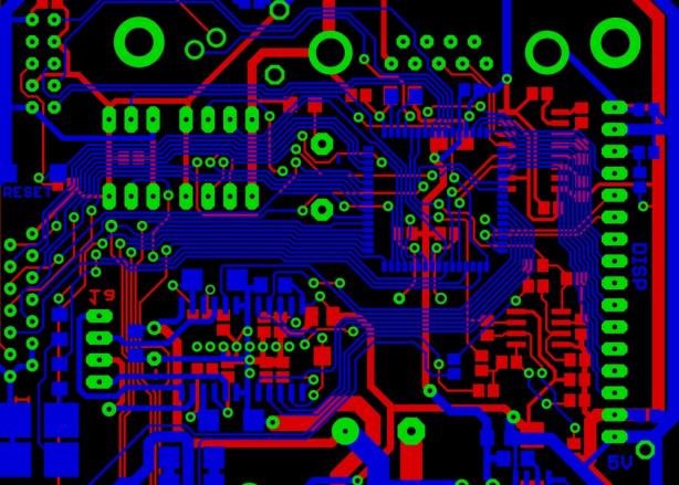
DFM in PCB design enhances the overall quality, cost-effectiveness, and efficiency of the product development process. It involves a holistic approach that spans various aspects of the design phase, benefiting manufacturers and end-users. The recent update expands checks to the populated circuit board, taking into consideration components and component placement data, over 150 DFA analysis items, and includes footprint and BOM checkers. With HQDFM, users can identify the exact location of highlighted issues in the simple interface, view the description and impact of the problem, and receive advice on how to address it.
During the PCB design process, the DFM principles help to produce high-quality, highly functional, and effective products. DFM principles can help manufacturers develop specifications in a functional layout, regardless of the dimensions of the printed circuit board (PCB).
Here is several ways how to apply DFM principles to PCBs:
- Component Placement Optimization: Proper component placement is vital for efficient PCB assembly. Components should be arranged to minimize signal interference, and thermal issues, and to facilitate automated assembly processes. Grouping components based on their functions and arranging them logically can streamline the assembly process.
- Design for Compliance and Safety: Ensuring that the PCB design complies with relevant regulations and safety standards is essential. This includes considerations such as spacing requirements for high-voltage components and EMI shielding to prevent interference with other electronic devices.
- Signal Integrity: The PCB layout design prevents electrical issues like interference and ensures signal integrity. This process is commonly known as electromagnetic interference or frequency interference.
- Optimize Trace Routing: Carefully designing the traces on the PCB to minimize signal interference, crosstalk, and impedance mismatches is essential. Proper trace routing can improve signal integrity and reduce the likelihood of manufacturing defects.
- Design for Soldering: Ensuring that components are properly soldered onto the PCB is critical for reliability. This involves selecting appropriate soldering techniques (e.g., reflow soldering, wave soldering) and designing pads and vias to facilitate solder flow and adhesion.
- Power and Ground Planes: Typically, the power and ground planes in PCB are wide traces of metal that are either connected to the standard connection or a power supply potential. They are used to reduce circuit noise.
- Material Section: Choosing the right materials for the PCB based on factors such as mechanical strength, thermal conductivity, and dielectric properties is important for both manufacturability and performance.
- Minimize the number of Unique Parts: Reducing the variety of components used in a PCB design simplifies procurement and inventory management. Standardizing components wherever possible can minimize costs and lead times.
HQDFM from NextPCB
NextPCB introduces HQDFM, a cutting-edge PCB Design Issue Detector and Solution Provider, engineered to streamline and enhance the accuracy of your PCB design process. HQDFM allows users to import their Gerber files with a single click, eliminating the complexities typically associated with file reading. This straightforward importing not only simplifies the process but also ensures that all necessary data for manufacturing is included in your design files. Additionally, the platform offers tools to easily visualize the complete design, helping to verify that every detail required for successful manufacturing is captured.
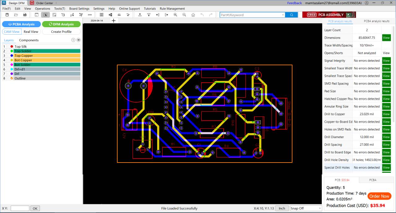
HQDFM is particularly adept at familiarizing users with Design for Manufacturability (DFM) protocols and production requirements. This feature is crucial for identifying potential manufacturing constraints early in the design process. The system provides a thorough check for hidden issues within the design, allows for the selection of compatible parts, and offers real-time cost evaluation. Furthermore, HQDFM enables the creation of personalized panels with precise control over the manufacturing specifics of both Surface Mount Technology (SMT) and through-hole components. Supported by a professional product and technical team, HQDFM offers tailored solutions that enhance design quality, performance, and reliability, thereby ensuring a smoother transition from design to production.
Conclusion
In conclusion, Design for Manufacturability (DFM) principles play a pivotal role in ensuring the success of PCB design end. By integrating DFM considerations into the design process, engineers can create PCB layouts that not only meet functional requirements but also streamline the manufacturing process, reduce costs, and enhance overall product quality. From optimizing component placement and trace routing to implementing design features for ease of assembly, testing, and thermal management, DFM principles empower designers to overcome manufacturing challenges and deliver robust, reliable PCB solutions. Top of Form The Design for Manufacturing (DFM) is essential for ensuring the production of profitable and outstanding PCB designs. Though the industry might face new miniaturization challenges, these challenges can be overcome by adopting automated and advanced techniques.
Moreover, the benefits of DFM extend beyond the manufacturing phase. By fostering collaboration between design and manufacturing teams early in the development cycle, DFM practices promote a holistic approach to PCB design that prioritizes efficiency, scalability, and innovation. Ultimately, embracing DFM principles not only ensures the successful realization of PCB designs but also fosters competitiveness, agility, and excellence in today’s rapidly evolving electronics industry.


