

In this article we will go through The History of Printed Circuit Board PCB from the timeline 1880 to Present. We will also see how PCB manufacturing is done by big PCB manufacturing giant like NEXTPCB. NextPCB comes under a parent company Shenzhen Huaqiu Electronics.
Overview
PCB stands for Printed Circuit Boards. Like other great inventions, PCBs also have their history from past to present. The printed circuit board (PCB) that we all know today was built on a foundation of advancements throughout history.
From the little corner of the world, we are able to trace the history of PCBs back over 130 years, when the great innovation of the industrial machine of the world was just started. What we’ll be covering in this blog isn’t an entire history, but rather the vast moments that transformed PCBs into what they’re today.
Evolution of PCBs
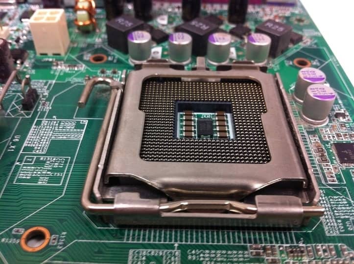
Over time, PCBs have evolved as an easy tool for optimizing the manufacturing of electronics products. What was once assembled easily by human hands soon gave the way to microscopic components which required the precision and efficiency of machinery. Consider the two circuit boards shown below. One is an older board for a calculator made within the 1960s. While the other is a typical high-density motherboard that you’ll see in today’s computers.

In the calculator, probably we can see 30+ transistors, but on a single chip motherboard, you can find millions of transistors. Actually, the rate at which technology and PCB design itself are advancing is really impressive. Everything that we saw on the PCB of the calculator can now fit into a single chip on today’s modern designs. Thus, huge noticeable trends are in the actions in the manufacturing of PCBs.
Let us go through the History of the Printed Circuit Board PCB Timeline from the 1880s to present-day PCB manufacturing and the changes that took place in between these years.
From 1880 to 1900
This was the time when electricity was brought into households, first starting in cities, then getting into the rural areas. Finally, Electricity was now an alternative to coal, wood, and oil. Electricity changed all of this. During this era major Inventions on electromagnetic & Motors took place.
Actually, this age was the period of genius inventors. Because it still has an impact on the electronics of today.
1. Thomas Alva Edison invented the lightbulb in 1879, known as America’s greatest inventor.
2. Nikola Tesla invented the motor in 1888 and AC power in 1895.
3. Alexander Graham Bell invented the telephone in 1876.
4. George Eastman’s Kodak invented the first consumer camera in 1884.
5. Herman Hollerith invented the tabulator in 1890 and would go on to found IBM.
One of the greatest Conflicts during this Age of innovation was between AC and DC. Nikola Tesla’s AC ended up winning out as only the method of transporting electricity over long distances. However, the interesting thing to note is how we’re still dealing with AC-DC conversion issues today.
Note: Actually, the beginning ideas for the PCB weren’t invented during this era. However, without the manufacturing progress of The Gilded Age, and also the spreading influence of electricity, the PCB would never be what it’s today.
From 1890 to 1920
This is the time that shows the primary patent for a PCB. In 1903, one of the famous German Inventor Albert Hanson filed a British patent for a device described as a flat, foil conductor on an insulating board having multiple layers.

Albert Hanson also described the whole concept hole application in his patent. He showed that we can punch a hole into the two layers and had perpendicular wires to establish electrical connectivity. The progressive Age marked the first World War. This conflict was purely focused on mechanical devices and the trench world war. Actually, the basic electronics, and even PCB concept, still hadn’t come into use in military applications, but they were evolving soon.
During 1920s
It was also during this time that we saw the invention of the trendy appliances we still rely on today like washing machines, vacuums, and refrigerators. But where are our PCBs? We’re still not seeing them utilized in any of the appliances or automobiles introduced during this age.
However, in 1925 Charles Ducas invented a patent that describes the way for adding conductive inks to an insulating material. this might later give birth to the printed wiring board (PWB). Actually, this patent was the first real application to relate a PCB. But was only used as a flat heating coil. We still haven’t got the actual electrical connectivity between board and components, but we’re getting closer to it.

During 1930-1945
This was the year noted as the most significant year in the History of Printed Circuit Board PCB. The second warfare is underway, and therefore the US enters the fray in 1942 after the bombing of Pearl Harbor. It was also during warfare 2 that we saw the first use of a PCB as we all know it today in the proximity fuse.
This device was used for high-velocity artillery shells, which needed to fireside precisely over massive distances in either sky or land. The proximity fuse was first Invented by the British to combat the push of Hitler’s Army.

During this time we even have Paul Eisler, an Austrian living within the UK, file a patent for copper foil on a non-conductive base of a glass. Sound familiar? This is often the concept we still use today for manufacturing PCBs with an insulating layer and copper on the top/bottom. Eisler took this concept one step further by making a radio along with his PCB in 1943, which might pave the way for future military applications.

During 1940s
Let’s see the history of Printed Circuit Board PCB during the 1940s. We see a lot of improvements to existing appliances like vacuum cleaners, washing machines, televisions, and radios. What we’re still not seeing though are consumer-level PCBs. Where is Paul Eisler’s work? Let’s have a look at this old television below, and you’ll see all of the components but no underlying PCB foundation.

Despite the shortage of PCBs, we did see the arrival of the transistor at Bell Labs in 1947.
From 1947 to 1970
Let’s move down to History of Printed Circuit Board PCB from 1947 to 1970. It’s the ERA where we see PCBs being used to their full potential. In 1956 the US Army released its patent for the “Processing of Assembling Electrical Circuits.” Now manufacturers had a technique to both hold electronics and establish connectivity between components with copper traces.
As PCBs start to take off in the manufacturing realm, we discover ourselves in the world’s first Space Race between the USA & Russia.

Back to PCBs, in 1963 we’ve Hazeltine Corporation filing a patent for the first plated through-hole technology. This is able to allow components to be closely spaced together on a PCB without concern about crossover connections. Actually, we also have seen the invention Surface Mount Technology (SMT) developed by IBM. These densely packed components found their first practical use in the Saturn rocket boosters.

The 1970s – The Dawn of the Microprocessor
The 70s brought us the first microprocessor within the sort of an integrated circuit (IC). This was firstly developed in 1958 by Jack Kilby at Texas Instruments.

It’s in the 1970s where we see ICs first being used within the manufacturing of electronics. Hence, from this time if you were not using a PCB board for connectivity you were in big trouble.
The 1980s – The Dawn of the Digital Age
The Digital Age brings about massive changes in how we consume media with the introduction of personal devices just like the CD, VHS, camera, gaming consoles, walkmans, etc.
It’s important to know that PCBs were still being drawn by hand with a light-weight board and stencils, then again computers and EDA arrived. Now we can see EDA software like Protel and EAGLE. It is completely changing how we design and manufacture electronics. Rather than photographs of PCBs, we’re now ready to save our designs as Gerber text files whose coordinates can easily be fed into manufacturing machinery to prepare a PCB.

The 1990s – The Internet Age
In the 90s we saw the utilization of silicon come with a full swing with the introduction of BGAs. Now we are able to fit more gates onto a single chip and begin to embed memories and Systems on Chip (SoC) together. This can be also a period of intense miniaturization in electronics. We don’t see any new features added to PCBs, but the whole design process is beginning to change and evolve, shifting to the IC.
Now designers need to implement Design for Test (DFT) strategies into their layouts. It’s not as easy as you think to pop off a component and add a blue wire. Engineers need to design their layouts from the perspective of future rework in mind. Are all of those components placed in a proper way that they can be easily removed? This is an enormous concern.
This is also a time where smaller component packages like 0402 make the hand soldering of boards nearly impossible. The designer now lives in his EDA software, and therefore the manufacturer handles the physical production and assembly.

The 2000s & Beyond – The Hybrid Age
We’re in an age of consolidation of devices, but what’s coming next? PCBs are established, we’ve processes and procedures for nearly everything. High-speed applications are getting the norm. We’re also seeing only 25% of PCB designers under the age of 45, and 75% are preparing to retire. The industry seems to be in an exceedingly period of crisis.


What is the future of PCB design in robotics? Maybe in wearables with flexible circuitry? Or perhaps we’d see protons replacing electrons with Photonics. As for the physical PCBs that we’ve come to know, even those might change within the future. rather than needing a physical medium for connectivity between components, there’s the potential for wave technology. This might allow parts to send signals wirelessly without having copper. That’s all from History of Printed Circuit Board PCB.
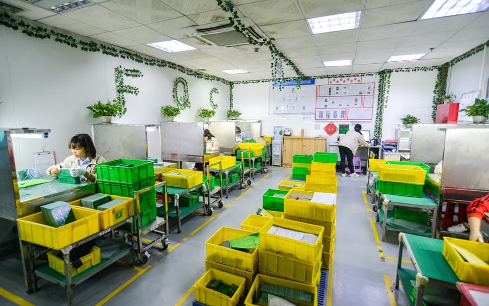
Modern Day PCB Manufacturing by NEXTPCB
About NEXTPCB
NextPCB is one of the most experienced PCB manufacturers in China, has specialized in the PCB and assembly industry for over 15 years, providing some of the most innovative printed circuit board with assembly technologies in terms of the highest quality standards, fastest delivery turnaround as fast as 24hours, lowest manufacturer direct prices, and the most dedicated customer service in the industry. You can count on NextPCB to meet your needs, from the simplest boards to the most complex designs for small quantity and large-scale production.

Services Provided by NEXTPCB
NextPCB provides the following services including sourcing components, PCB prototyping, PCB manufacturing, PCB assembly, quality testing, and the final shipment.

You can visit their official website to learn more about their services. Check it here: https://www.nextpcb.com/.
PCB Manufacturing Process by NEXTPCB
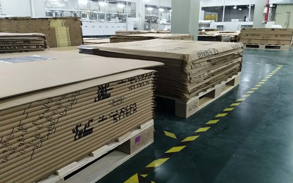
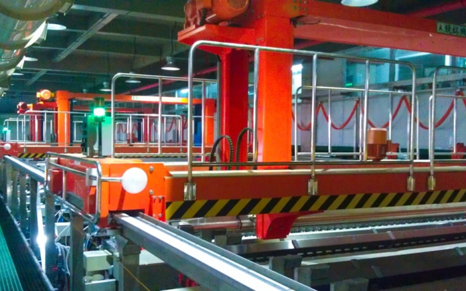
The PCB manufacturing process is a very long process and requires a lot of time. But NextPCB has all the latest modern machinery and tools that will make the prototype ready in 24 hours. The PCB manufacturing includes the following steps.
1. Pre-Product Engineering
2. Board Cutting
3. Drilling
4. Deburr
5. Electroless Copper Deposition
6. Copper Plate Making
7. Image Expose
8. Image Develop
9. Inner Layer Etch
10. Automatic Optical Inspection (AOI)
11. Solder Mask Applications
12. Bake
13. Rescue Solder Pad
14. Legend
15. Surface Finish
16. Electrical Test
17. Outline Process – Rout, v-scoring
18. Wash Boards
19. Final Inspection


Once the PCB manufacturing process is completed, the assembly services need to be done. The PCBA services include the following process.
1. Components Checking
2. Solder Paste Printing
3. Pick & Place SMD Parts
4. Reflow Soldering
5. Flipping
6. THT Component Placement
7. Wave Soldering (hand soldering)
8. AOI Checking/ X-Ray
9. Visual Inspection (Repairing)
10. Quality Control/Packaging
11. Delivery.
The complete PCB Manufacturing Process is explained in the video below.

You can also etch the PCB at home using 3D Printer PCB Etching method easily.
How to place a PCB/PCBA order from NextPCB?
If you want to order the PCB and PCBA services from the NEXTPCB, you can follow the video below.

PCB Samples and Assembled Boards
I have added few samples of PCB and assembled boards from NextPCB. The PCB quality is brilliant and superb. The services and facilities provided by them are up to the mark and best. Compared to all other PCB manufactures, I will personally recommend NextPCB to all the project lovers and industrialist.


The History of Printed Circuit Board PCB from timeline 1880 to Present is very interesting as you read above. From the old PCB designing methods back in 1960 to modern-day EDA tools for PCB Designing with NextPCB took so many inventions and technology setup.


