

Introduction
A rectifier that converts the complete cycle of alternating current (AC) into direct current (DC) or pulsating DC is called Full Wave Rectifier. In this type of rectifier, both the positive and negative half cycle of the AC input signal can be rectified. During construction, a full wave rectifier uses multiple diodes or groups of diodes for the rectification process.
The working of a full wave rectifier is also based on the fact that the diode allows current flow in one direction and blocks the current in another direction. In a full wave rectifier, the current flows through the load in the same direction for the complete cycle of the input AC supply.
The full wave rectifier is mainly designed to overcome the drawback of a half-wave rectifier such as power loss, low efficiency, and higher ripple factor. It produces the DC output voltage which is higher than the half wave rectifier. The output of a full wave rectifier has less amount of ripple than that of a half-wave rectifier. Hence full wave rectifier produces a smoother output DC waveform and gives higher efficiency.
The full wave rectifier is further classified into two types. They are:
- Center Tapped Full Wave Rectifier
- Full Wave Bridge Rectifier
Center Tapped Full Wave Rectifier
A type of full wave rectifier that uses two diodes connected to the secondary winding of the center-tapped transformer is called center tapped full wave rectifier. The center-tapped full wave rectifier mainly consists of the following components.
- Center tapped Transformer
- Two diodes
- Resistive Load
The circuit diagram for center tapped full wave rectifier is shown in the figure below.

In this circuit, the input AC supply is connected to the primary winding of the center–tapped transformer. In the secondary winding of the transformer, a center tap (additional wire) is connected at the exact center point so that the center tap divides the input into two parts. The upper part of the secondary winding is connected to the diode and the lower part of the secondary winding is connected to the diode. Both the diodes are connected to the common resistive load with the help of the center tap transformer as shown in the above figure.
Operation of Center Tapped Full Wave Rectifier
During the positive half cycle of AC supply, terminal A becomes positive and terminal B becomes negative. The center tap is grounded i.e. it is at zero potential. Here, the positive terminal is connected to the p side of the diode, and negative terminal B is also connected to the p side of the diode. So that the diode is in forward biased condition and allows the flow of current through. Whereas the diode is in reverse biased condition and does not allow electric current through. Hence diode supplies DC current to the load and it will be returned to the secondary winding of the transformer. The current flows in the path of the line arrow as shown in the figure.
During the negative half cycle of AC supply, terminal A becomes negative and terminal B becomes positive. The center tap is grounded i.e. it is at zero potential. Here, negative terminal A is connected to the p side of the diode and the positive terminal B is connected to the p side of the diode. So that the diode is in reverse biased condition and does not allow electric current through whereas the diode is in forward biased condition and allows the flow of current through Hence diode supplies DC current to the load and it will be returned to the secondary winding of the transformer. The current flows only in the lower part of the circuit. The current flows in the path of the dotted line arrow as shown in the figure.
From both half cycles of AC supply, it is observed that the diode allows electric current during the positive half cycle and the diode allows electric current during the negative half cycle. Thus the input AC signal is allowed for both positive and negative half cycles. The current flows in the same direction across the load. The output DC voltage is almost equal to the input AC supply voltage.
The input-output waveform of a center tapped full wave rectifier is shown in the figure below:

Full Bridge Rectifier
A type of full wave rectifier that uses four diodes in a bridge formation is called a full wave bridge rectifier. Four diodes are connected in a bridge fashion in which two diodes conduct for one-half cycle and the other two diodes conduct for another half cycle.
A full wave bridge rectifier does not require any center tap and a center-tapped transformer. So it is less costly and smaller in size than center tapped full wave rectifier.
The Full Wave Bridge Rectifier mainly consists of the following components.
- Four diodes
- Resistive Load
The circuit diagram for the Full Wave Bridge Rectifier is shown in the figure below.

In this circuit, four diodes are arranged to form a bridge. The AC supply or output of the transformer at the secondary winding is connected to two diametrically opposite points of the bridge at points A and C. The resistive load is connected to the bridge through points B and D. The connection of AC supply, diodes as a bridge, and load resistance is shown in the figure above.
Operation of Full Wave Bridge Rectifier
During the positive half cycle of AC supply, the upper terminal A of the bridge is positive with respect to the lower terminal C. Thus, the diodes are in forward biased condition, and current flows to the load resistance through arm AB and returns back flowing through arm DC. Whereas diodes are in reverse biased condition and current is not allowed to flow in arms AD and BC.
The circuit diagram during a positive half cycle is shown in the figure below and the path of the flow of current is indicated by arrows. In this half cycle, the current flows through the path AB-RL- DC and completes the circuit as shown in the figure.

During the negative half cycle of AC supply, the upper terminal A of the bridge is negative with respect to the lower terminal C. Thus, the diodes are in reverse biased condition and current is not allowed to flow in arms AB and DC. Whereas diodes are in forward biased condition and current flows to the load resistance through arm CB and return back flowing through arm DA.
The circuit diagram during a negative half cycle is shown in the figure below and the path of the flow of current is indicated by arrows. In this half cycle, the current flows through the path CB-RL – DA and completes the circuit as shown in the figure.

The input-output waveform of the full wave bridge rectifier is shown in the figure below:

Ripple Factor of Full Wave Rectifier
The direct current (DC) produced by a full wave rectifier is not a pure DC but a pulsating DC. There are some AC components remaining when converting the AC signal to DC signal even though we try out best to remove AC components. This unwanted AC component contained in the output side of the rectifier is called a ripple. The ripples in the output DC signal can be minimized by using filters such as capacitors and inductors.
The ripple factor gives the number of ripples present in the output DC signal. It is used to measure how well the half-wave rectifier can convert ac voltage into DC voltage. Mathematically, the ripple factor is the ratio of the RMS value of the AC component of output voltage to the DC component of output voltage. Or it is the ratio of ripple voltage to the DC voltage.
For the construction of a good rectifier, the ripple factor should be kept as minimum as possible. Thus, capacitors and inductors are used as filters to reduce the ripples in the circuit.
The ripple factor is denoted by γ and is given by the formula:
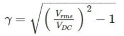
For center tapped full wave rectifier, the ripple factor comes out to 0.48.
![]()
RMS Value
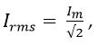
The RMS value of current flowing through the load resistance RL for full wave rectifier is given as:
The RMS value of output load voltage is given by:
![]()
Output DC Voltage (Vdc)
The Output DC Voltage (Vdc) is the voltage appeared across the load RL. This is obtained by the multiplication of output dc current and load resistance RL.
Mathematically it can be written as:
![]()
The Output DC Voltage (Vdc) is given by:
![]()
Efficiency
The efficiency of the rectifier is the ratio of output dc power to the input ac power. It is denoted by ղ and mathematically written as:
![]()
For a Full Wave Rectifier, The efficiency is equal to 81.2% which is twice the efficiency of the half-wave rectifier.
Peak Inverse Voltage (PIV)
Peak inverse voltage (PIV) is the maximum reverse bias voltage that the diode can withstand. The diode will be destroyed if an applied voltage is greater than the peak inverse voltage (PIV).
The peak inverse voltage of a full wave rectifier is double that of a half wave rectifier. The PIV across is D1 & D2 is 2Vmax.
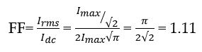
Form Factor
The form factor is defined as the ratio of RMS value to the DC value or average value. Mathematically, it is given as:
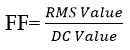
For full Wave rectifier, the form factor is:
Applications
The full wave rectifier is mainly used for the following applications:
- They are used for identifying the amplitude of modulating radio signal
- Full wave bridge rectifiers are sued in a power supply circuit for different applications.
- They are used to provide power supply to devices that require DC voltage similar to LED and motor.
- They are used in mobile phones, laptops, and charger circuits.
- They are used in UPS to convert AC into DC.
- They are used in welding.
Adavantages
The main advantages of a full wave rectifier are as follows:
- They have higher efficiency than half-wave rectifiers. i.e. they convert AC into DC more efficiently.
- There is no loss in output power since they utilize both half cycles and no voltage signal is wasted in the rectification process.
- They have less ripple factor. i.e. output voltage of full wave rectifier has lower ripples than half wave rectifier.
Disadavantages
The disadvantages of a full wave rectifier are as follows:
- They need more circuit elements than half wave rectifiers which makes them complex and tends to occupy a lot of space.
- They are more expensive than half-wave rectifiers.


